EFFECT Photonics Tapes out World’s First full Photonic Integration Coherent PIC
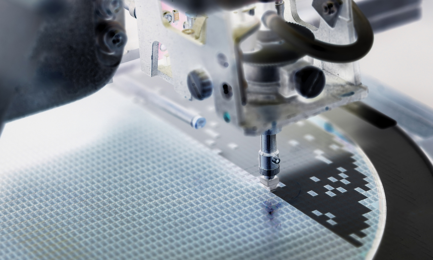
Building on its Full Photonic Integration InP wafer scale platforms, EFFECT Photonics has taped out the Manta chip: the world’s first fully integrated coherent PIC targeted at pluggable coherent transceivers for the edge and metro/access networks.
The Manta PIC fully integrates an ultra-narrow linewidth full band tunable laser, 64Gbaud coherent receiver, 64Gbaud coherent transmitter, wavelength locking and on-chip amplification for the transmit and receive paths. This gives unprecedented OSNR performance with power consumption lower than a stand-alone ITLA.
Tim Koene, VP Engineering at EFFECT Photonics, describes the benefits of the approach: “Full Photonic Integration means including all of the needed functions for coherent. In some approaches, the most costly functionalities, notably the laser, amplification and wavelength locking, are not integrated, and this creates optical loss, higher cost and higher assembly complexity. Truly integrating everything allows us to overcome those hurdles and create a high-performance, low-power consumption, low-cost solution for coherent.”
EFFECT Photonics will build small form-factor coherent pluggables optimised for industrial temperature operation. They will be deployed in next generation access networks and be able to provide turnkey coherent transmission over 120km of unamplified links.
James Regan, CEO at EFFECT Photonics, comments on the achievement: “Being able to deliver this single-chip solution in the same industrial-temperature specification, non-hermetic platform, with which we are shipping our tunable SFP+ targeting 5G wireless connectivity, is a game changer. It enables us to execute on our strategy and take the benefits of coherent technology closer than has been possible before to the end user in high-volume applications.”
The Manta PIC is fabricated on EFFECT Photonics’ 3″ InP platform and will be ported to 4″ fabrication later this year. It is set to drive a revolution in cost optimisation for the next generation of coherent networks.
-End-
About EFFECT Photonics
EFFECT Photonics delivers highly integrated optical communications products based on its Dense Wavelength Division Multiplexing (DWDM) optical System-on-Chip technology. The key enabling technology for DWDM systems is full monolithic integration of all photonic components within a single chip and being able to produce these in volume with high yield at low cost. With this capability, EFFECT Photonics is addressing the need for low cost DWDM solutions driven by the soaring demand for high bandwidth connections between datacenters and back from mobile cell towers. Headquartered in Eindhoven, The Netherlands, with additional R&D and manufacturing in South West UK, with sales partners worldwide. www.effectphotonics.com
For further information please contact sales@effectphotonics.com